Epitaxial growth, often also referred to as epitaxy, is one of the most important processes in the fabrication of semiconductor materials and devices. The so-called epitaxial growth is in certain conditions in the single crystal substrate on the growth of a layer of single product film process, the growth of single-crystal film is called epitaxial layer epitaxial technology is the early 1960s in the silicon single-crystal thin film research on the basis of the emergence of the development of nearly half a century now, people have been able to realize a variety of semiconductor films under certain conditions of epitaxial growth. Epitaxial technology has solved many problems in semiconductor discrete components and integrated circuits, greatly improving the performance of the device. Epitaxial film can more accurately control its thickness and doping properties, this feature has led to the rapid development of semiconductor integrated circuits, into a more perfect stage. Silicon single crystal by slicing, grinding, polishing and other processing techniques, to get polished sheet, you can make discrete components and integrated circuits on it. But in many occasions this polished sheet only as a mechanical support for the substrate, in which it is necessary to first grow a layer of single-crystal film with the appropriate type of conductivity and resistivity, and then discrete components or integrated circuits produced in a single-crystal film. This method is used, for example, in the production of silicon high-frequency high-power transistors, resolving the conflict between breakdown voltage and series resistance. The collector of the transistor requires a high breakdown voltage, which is determined by the resistivity of the p-n junction of the silicon wafer. In order to meet this requirement, high resistance materials are required. People in the heavily doped n-type low-resistance materials on the epitaxial several to a dozen microns thick lightly doped high-resistance n-type layer, transistor production in the epitaxial layer, which solves the high breakdown voltage required by the high resistivity and low collector series resistance required by the low substrate resistivity of the contradiction between.
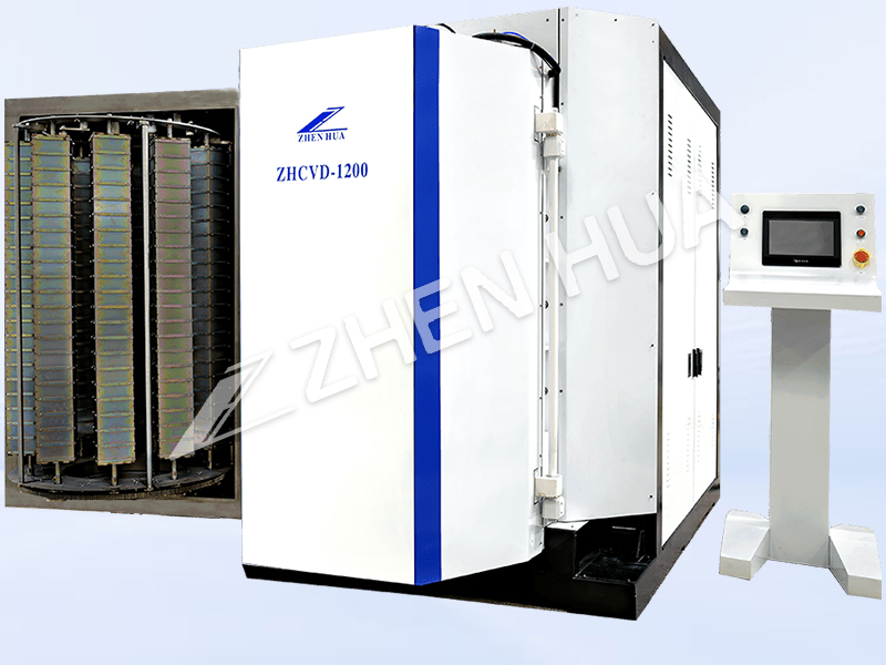
Gas-phase epitaxial growth is the earliest application in the semiconductor field of a more mature epitaxial growth technology, which plays an important role in the development of semiconductor science, greatly contributing to the quality of semiconductor materials and devices and their performance improvement. At present, the preparation of semiconductor single crystal epitaxial film is the most important method of chemical vapor deposition. The so-called chemical vapor deposition, that is, the use of gaseous substances on the solid surface of the chemical reaction, the process of generating solid deposits. CVD technology can grow high-quality single-crystal films, to obtain the required doping type and epitaxial thickness, easy to realize the mass production, and therefore has been widely used in industry. In industry, the epitaxial wafer prepared by CVD often has one or more buried layers, which can be used to control the device structure and doping distribution by diffusion or ion implantation; the physical properties of CVD epitaxial layer are different from those of the bulk material, and the oxygen and carbon content of the epitaxial layer is generally very low, which is its advantage. However, CVD epitaxial layer is easy to form self-doping, in practical applications need to take certain measures to reduce the epitaxial layer of the self-doping, CVD technology is still in some aspects of the empirical process state, need to do more in-depth research, so that it continues to get the development of the CVD technology.
CVD growth mechanism is very complex, in the chemical reaction usually includes a variety of components and substances, can produce a number of intermediate products, and there are many independent variables, such as temperature, pressure, gas flow rate, etc., epitaxial process has a number of back and forth successively, each other to develop and improve. The epitaxial process has many successive, mutually expanding and perfecting steps. To analyze the process and mechanism of CVD epitaxial growth, first of all, to clarify the solubility of reactive substances in the gas phase, the equilibrium partial pressure of various gases, clear kinetic and thermodynamic processes; then to understand the reactive gases from the gas phase to the surface of the substrate mass transport, the formation of the boundary layer of the gas flow and the surface of the substrate, the growth of the nucleus, as well as the surface reaction, diffusion and migration, and thus ultimately generate the desired film. In the growth process of CVD, the development and progress of the reactor play a crucial role, which largely determines the quality of the epitaxial layer. The surface morphology of the epitaxial layer, lattice defects, distribution and control of impurities, thickness and uniformity of the epitaxial layer directly affect the device performance and yield.
–This article is released by vacuum coating machine manufacturer Guangdong Zhenhua
Post time: May-04-2024


