
In the modern electronics industry, ceramic substrates are widely used as essential electronic packaging materials in power semiconductors, LED lighting, power modules, and other fields. To enhance the performance and reliability of ceramic substrates, the DPC (Direct Plating Copper) process has emerged as a highly efficient and precise coating technology, becoming a core process in ceramic substrate manufacturing.
No.1 What is the DPC Coating Process?
As the name suggests, the DPC coating process involves directly coating copper onto the surface of a ceramic substrate, overcoming the technical limitations of traditional copper foil attachment methods. Compared to conventional bonding techniques, the DPC coating process significantly improves the adhesion between the copper layer and the ceramic substrate while offering higher production efficiency and superior electrical performance.
In the DPC coating process, the copper coating layer is formed on the ceramic substrate through chemical or electrochemical reactions. This approach minimizes delamination issues commonly seen in traditional bonding processes and allows for precise control over electrical performance, meeting increasingly stringent industrial demands.
No.2 DPC Coating Process Flow
The DPC process consists of several key steps, each critical to the quality and performance of the final product.
1. Laser Drilling
Laser drilling is performed on the ceramic substrate according to design specifications, ensuring precise hole positioning and dimensions. This step facilitates subsequent electroplating and circuit pattern formation.
2. PVD Coating
Physical Vapor Deposition (PVD) technology is used to deposit a thin copper film on the ceramic substrate. This step enhances the electrical and thermal conductivity of the substrate while improving surface adhesion, ensuring the quality of the subsequent electroplated copper layer.
3. Electroplating Thickening
Building on the PVD coating, electroplating is used to thicken the copper layer. This step strengthens the durability and conductivity of the copper layer to meet the demands of high-power applications. The thickness of the copper layer can be adjusted based on specific requirements.
4. Circuit Patterning
Photolithography and chemical etching techniques are used to create precise circuit patterns on the copper layer. This step is crucial for ensuring the electrical conductivity and stability of the circuit.
5. Solder Mask and Marking
A solder mask layer is applied to protect non-conductive areas of the circuit. This layer prevents short circuits and enhances the insulation properties of the substrate.
6. Surface Treatment
Surface cleaning, polishing, or coating treatments are performed to ensure a smooth surface and remove any contaminants that could affect performance. Surface treatments also improve the corrosion resistance of the substrate.
7. Laser Shaping
Finally, laser processing is used for detailed finishing, ensuring that the substrate meets design specifications in terms of shape and size. This step provides high-precision machining, especially for complex-shaped components used in electronic and interior applications.
No.3 Advantages of the DPC Coating Process
The DPC coating process offers several significant advantages in ceramic substrate production, including:
1. High Adhesion Strength
The DPC process creates a strong bond between the copper layer and the ceramic substrate, greatly improving the durability and peel resistance of the copper layer.
2. Superior Electrical Performance
Copper-plated ceramic substrates exhibit excellent electrical and thermal conductivity, effectively enhancing the performance of electronic components.
3. High Precision Control
The DPC process allows precise control over copper layer thickness and quality, meeting the stringent electrical and mechanical requirements of various products.
4. Environmental Friendliness
Compared to traditional copper foil bonding methods, the DPC process does not require large amounts of harmful chemicals, making it a more environmentally friendly coating solution.
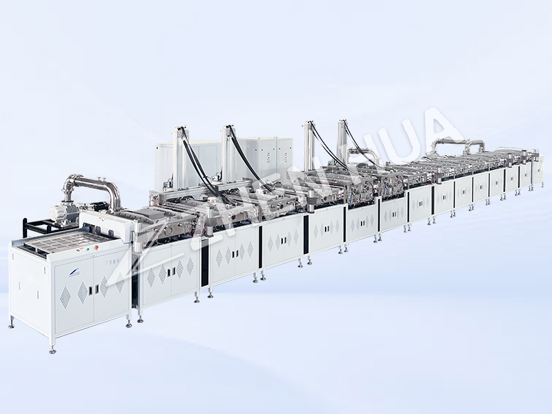
4. Zhenhua Vacuum’s Ceramic Substrate Coating Solution
DPC Horizontal Inline Coater, Fully Automated PVD Inline Coating System
Equipment Advantages:
Modular Design: The production line adopts a modular design, allowing for flexible expansion or reduction of functional areas as needed.
Rotating Target with Small-Angle Sputtering: This technology is ideal for depositing thin film layers inside small-diameter holes, ensuring uniformity and quality.
Seamless Integration with Robots: The system can be seamlessly integrated with robotic arms, enabling continuous and stable assembly line operations with high automation.
Intelligent Control and Monitoring System: Equipped with an intelligent control and monitoring system, it provides comprehensive detection of components and production data, ensuring quality and efficiency.
Application Scope:
It is capable of depositing a variety of elemental metal films, such as Ti, Cu, Al, Sn, Cr, Ag, Ni, etc. These films are widely used in semiconductor electronic components, including ceramic substrates, ceramic capacitors, LED ceramic brackets, and more.
— This article is released by DPC copper deposition coating machine manufacturer Zhenhua Vacuum
Post time: Feb-24-2025